Main progress achieved in Europe (since end 2021)
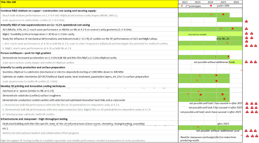
Continue R&D niobium on copper. Reach bulk niobium performances on 1.3–0.4 GHz elliptical and various cavity shapes. Up to now, only CERN has a systematic program for depositing cavities with various frequencies and shape. INFN, STFC/CI and USI also have activities in that domain. One has now a better understanding of the role of the copper substrate quality (smoothness, surface treatment at INFN, HZDR and RTU , interlayers at CEA) and of the density of the film to ensure success. R&D is still necessary to fully optimize the process and increase the production yield.
Intensify R&D of new superconductors on Cu.– Reach same performance as Nb3Sn on Nb at 4.2 K on several cavity geometry (1.3–0.6 GHz).Several efforts have been done in depositing Nb3Sn (CERN, INFN, STFC), or NbTiN and NbN (CEA, H.U., USI, STFC) on copper substrates. STFC is the only lab that has attempted to work on MgB2. Several difficulties still need to be explored. For instance, there are issues with tin diffusion in the copper substrate, or tin evaporation during heat treatments. Several routes needs to be explored (e.g. interlayer between copper and the superconducting layer at CEA, or compounds from the same family -V3Si- which should be less sensitive to evaporation at STFC). Studying the influence of mechanical deformations and trapped flux sensitivity also need to be complete. First attempts to deposit inside cavities (split cavities, 6 GHz) are on going at STFC and INFN.
Pursue multilayers. Demonstrate increased acceleration on 1.3 GHz bulk Nb and thin-film Nb/Cu 1.3 GHz elliptical cavity. For now CEA, H.U., STFC and USI have deposited and characterized ML samples. CEA and HU have developed cavity deposition set-ups based on ALD (atomic layer deposition) and are in the process of transferring the technology to deposit in the first prototype cavities.
Intensify Cu cavity production and surface preparation Optimize air stable chemistries (EP-BCP/without liquid waste, heat treatment, passivation layers, etc.) for Cu surface preparation. CERN is exploring several fabrication routes while INFN developed an automated production process (by spinning) with the company Piccoli. INFN is also involved in surface treatment by plasma electropolishing with promising results. Other surface treatments processes are being explored (laser treatment at RTU, Flash annealing at HZDR, mechanical-chemical polishing by IJCLab with CEA…), but it is still at small scale.
Develop 3D printing and innovative cooling techniques. Demonstrate substrate (cavities) surface roughness. Demonstrate conduction cooled cavities. Additive manufacture activities are undertaken at CEA, CERN and INFN. CEA demonstrated a Cryocooled 3D printed doubled walled 3.9 GHz cavity, one 1 µm roughness on samples, but activity is stopped for lack of resources. INFN has developed a protocol to produce 6GHz cavities with subsequent surface treatment and final roughness below 400 nm. They are also AM activities at CERN, but not directly related to thin film deposition goals.
Infrastructures and manpower, high-throughput testing. Since 2021, most of the labs have been commissioning their deposition set-ups for 6 GHz cavities and started development for 1.3 GHz deposition: HIPIMS at CERN, HPCVD, DCMS, HIPIMS in STFC, DCMS at INFN, HIPIMS at USI, and as said previously 1.3 GHz ALD set-ups at CEA and HU.
Specific measurement set-ups have been developed or further improved (e.g. full field penetration experiments at STFC, tunneling microscopy at CEA). Concerning sample RF characterization, another QPR cavity has been commissioned at Desy( HU), a choke 7.8 TM GHz cavity has been developed at STFC, and an TM020 4.8 Ghz cavity has been developed at HZB in addition to their QPR.
The construction of a dedicated building (surface preparation, thin film deposition, cleanroom…) is being foreseen for the end of the decade at CERN.
